About
I am currently a Product Development Engineer at Intel, where I serve as the key technical liaison between high-volume production fabs, design teams, and other corporate entities. I have led the product development of server SoCs, including Xeon, Sapphire Rapids, and have extensive experience in Intel 7 and Intel 3 technology nodes (transistor development). My expertise includes nanofabrication, semiconductor physics, and process optimization, with a focus on improving yields and operational efficiency. I have also worked on advanced projects like CubeSat research for NASA -WV robotic station and am skilled in applying SPC and DOE techniques for quality control.
Additional research areas: Machine Learning, Artificial Intelligence, Circuit designing, AI robotics, Image processing, Semiconductor physics, Nano-fabrication, Photonic and Plasmonic nanostructures, Biosensors, Device physics, Electrochemistry, Solar energy and FDTD simulations.
Education
West Virginia University (WVU) – Morgantown, WV, USA
Research: Developing plasmonic nanostructures for bio-sensing and light management applications.
Advisor: Dr.Nianqiang Wu
West Virginia University (WVU) – Morgantown, WV, USA
Research: Improving GaN LED performance by analyzing MOCVD grown GaN defects using transient spectroscopies (CV and DLTS).
Advisor: Dr.Lawrence Hornak
Andhra University(SRKR) – Visakhapatnam, A.P, India
Electronics and Communication Engineering
Experience
As Lead Engineer for Sapphire Rapids product, I managed the transition from NPI to production, optimizing wafer utilization and saving $4.8M through demand-driven adjustments. I collaborated with cross-functional teams to improve power, performance, and yield, ensuring testability and manufacturability from feasibility to production ramp. I provided strategic guidance on component performance and identified improvement opportunities, enhancing production efficiency.
I led scientific research and development in semiconductor manufacturing, optimizing advanced device architectures and improving yield, quality, and reliability. With expertise in P1276/78 Dry Etch TEL tools for 7/5nm technology, I reduced Tri-layer etch process run time by half, enhancing equipment utilization. I also predicted dry pump failure rates using statistical analysis, saving $1M in maintenance costs. I managed a 24x7 technician team, implemented process controls (APC, SPC, PCS), and developed defect-free process conditions to boost efficiency and equipment reliability.
At WVU, I worked in the Bio-sensing, Bio-imaging, and Nano-toxicity Lab, where I developed a novel fabrication process for creating large-area gold-coated silicon nano-ring arrays for SERS and point-of-care biosensors. I also analyzed their optical properties using FDTD simulations. In the Solar Energy Conversion Lab, I focused on tuning the plasmonic properties of 3D nanostructures to improve solar energy conversion efficiency and maintained Surface Photo Voltage Spectroscopy (SPV) for semiconductor surface characterization.
Worked on cube-sat project where -Hands on experience on vacuum and low temperature systems. Experienced in analyzing the C-V and DLTS signals for quantifying doping concentration, activation energy of traps, and traps concentration of group III-V semiconductors. Maintained communication between growth and characterization groups for GaN purity feedback.
establishments
We are a leading provider of custom application, end-to-end IT service and an innovative electronics and software product development company. SINFOTECH was founded in 2021 in West Virginia-USA, is a provider of Custom Application Development and end-to-end IT Services to clients globally. We use a client-centric engagement model that combines local on-site and off-site resources with the cost, global expertise and quality advantages of off-shore operations. We deliver Custom Application Development, innovative electronics and software product development, Application Modernization, Business Process Outsourcing and Professional IT Services from office locations in the USA and India.
link:sinfotech
We develop high quality bespoke web and mobile applications for organizations, institutions and SMEs Our team is well vast in software development and is ready to help develop the applications of your choice. We take responsibility for building custom software solutions that caters for automation of your business processes and improve efficiency.
Link:Everlytech
Safetax is a dedicated tax filing company offering personalized tax filing services to individuals. Known for its commitment to security, Safetax ensures that all client documents are transferred through secure, encrypted channels, prioritizing data privacy and confidentiality. With an emphasis on accuracy and compliance, the company keeps up-to-date with the latest tax regulations to provide timely, reliable guidance, minimizing clients' tax liabilities while maximizing eligible deductions. Safetax also offers responsive customer support, assisting clients at every stage of the filing process to make tax season as smooth and stress-free as possible.
Link:
Elsoftron Tech, established in 2021 in Andhra Pradesh, India, is a dynamic software and research company dedicated to advancing electronics and Artificial Intelligence. As a sister company to Sinfotech LLC in the USA, Elsoftron Tech not only provides outsourced software services but also fosters innovation through collaborative research with SRKR College. This partnership positions the company as a leading hub for technology-driven research and development, bridging expertise between India and the USA
Link:
Skills
Fabrication Tools
- Reactive Ion Etching (Trion Technology Minilock III RIE)
- Sputter deposition (CVC 610DC Magnetron sputtering station)
- Spin coating (Laurel technologies 400 spinner)
- UV Lithography (Suss Microtech MA6 Aligner)
- Flood exposure (OAI UV Flood exposure)
- Gold Wire Bonder (West Bond 74776E)
- Rapid Thermal Processing (AnnealSys AS-Micro RTA)
- Oxygen Plasma Asher (March PX-250 Plasma Asher)
- E-beam evaporation (BOC Temescal BJD- 2000, Kurt J Lekser LAB18)
Characterization tools
- Scanning Electron Microscope (JEOL JSM-7600F SEM)
- Stylus Profilometer (Tencor Alpha-Step 200)
- Optical spectrum analyzer (Ocean optics USB 4000)
- Lock-in amplifier (SR 850)
- Raman spectrum analyzer (iRaman plus B&W Tek)
- Current-Voltage(I-V)
- Atomic Force Microscope (Nanoscope, AFM)
- Hall effect measurements, Capacitance-Voltage(C-V)
- Deep Level Transient Spectroscopy (DLTS)
- Surface Photo Voltage (SPV)
Publications
1.Kasani Sujan, Peng Zheng, and Nianqiang Wu. "Tailoring optical properties of a large-area plasmonic gold nanoring array pattern." The Journal of Physical Chemistry C 122.25 (2017): 13443-13449. (Invited)
Abstract
A new fabrication route, which combines nanosphere lithography>with silicon-based clean-room microfabrication processes, has been developed to produce large-area long-range ordered gold nanoring array patterns in a controllable fashion. Both the experimentation and the finite-difference time-domain (FDTD) simulation show that the surface plasmon resonance peak (SPR) of the nanoring array pattern can be tuned systematically in a large spectral range by varying the geometry parameters such as the ring thickness, the ring height, the ringer outer diameter, and the gap between neighboring rings. For the Au nanoring arrays with a large gap in the absence of plasmon coupling between neighboring rings, the local electromagnetic (EM) field enhancement occurs at both the outer and inner surfaces of individual nanorings; and the periodicity of Au nanoring array has no any effect on the plasmonic properties. For the Au nanoring arrays with a small gap, plasmon coupling takes place between neighboring rings. As a result, the characteristic plasmonic band is split into two new peaks corresponding to a bonding SPR mode and an antibonding SPR mode. The local EM field enhancement becomes stronger with a decrease in the gap between neighboring rings, but the SPR peaks shift away. Therefore, to maximize the surface- enhanced Raman scattering signal, the geometry parameters of the Au nanoring array need to be tuned to balance the contributions from the resonance excitation(spectral overlap) and the local EM field enhancement.
2.Zheng, Peng, Sujan Kasani (co-first author), and Nianqiang Wu. "Converting plasmonic light scattering to confined light absorption and creating plexcitons by coupling a gold nano-pyramid array onto a silica–gold film." Nanoscale Horizons 4.2 (2019): 516-525.
Abstract
This report presents a facile microfabrication-compatible approach to fabricate a large area of plasmonic nano- pyramid array-based antennas and demonstrates effective light management by tailoring the architecture. First, a long-range ordered gold nano- pyramid array is fabricated, which exhibits strong light scattering. The maximum electric field enhancement (|E|/|Eol) of 271 is achieved at the corner but decays rapidly away from the ne pyramid bottom. After the gold nanopyramid array is coupled to a gold film, strong light scattering is converted into strong light absorption due to the excitation of a spectrally tunable plasmonic gap mode, where an intense electric field enhancement of 233 and a strong magnetic field enhancement (|H|/|Hol) of 25 are simultaneously excited for a 10 nm silica gap. The electric field decays much slower away from the pyramid bottom while the magnetic field keeps almost constant. In addition, both experiments and finite-difference time-domain (FDTD) simulations have confirmed that strong plasmon-exciton coupling between the plasmonic gap mode and the J-aggregates can take place when quantum emitters such as J-aggregates are embedded in the gap, creating plexcitons. This can overcome the problems of high energy loss and weak nonlinearity, which are typically associated with surface plasmon polaritons (SPPs) supported on plasmonic metallic nanostructures. The coherent plasmon-exciton coupling (plexciton) generated by the film-coupled nano-pyramid nanostructure is expected to find promising applications in light-emitting devices, photodetectors, photovoltaics and photoelectrochemical cells.
3.Kasani Sujan, Kathrine Curtin, and Nianqiang Wu. "A review of 2D and 3D plasmonic nanostructure array patterns: fabrication, light management and sensing applications." Nanophotonics (2019) (Invited)
Abstract
This review article discusses progress in surface plasmon resonance (SPR) of two-dimensional (2D) and three-dimensional (3D) chip-based nanostructure array patterns. Recent advancements in fabrication techniques for nano-arrays have endowed researchers with tools to explore a material's plasmonic optical properties. In this review, fabrication techniques including electron-beam lithography, focused-ion lithography, dip-pen lithography, laser interference lithography, nanosphere lithography, nanoimprint lithography, and anodic aluminum oxide (AAO) template-based lithography are introduced and discussed. Nano- arrays have gained increased attention because of their optical property dependency (light-matter interactions) on size, shape, and periodicity. In particular, nano-array architectures can be tailored to produce and tune plasmonic modes such as localized surface plasmon resonance (LSPR), surface plasmon polariton (SPP), extraordinary transmission, surface lattice resonance (SLR), Fano resonance, plasmonic whispering-gallery modes (WGMs), and plasmonic gap mode. Thus, light management (absorption, scattering, transmission, and guided wave propagation), as well as electromagnetic (EM) field enhancement, can be controlled by rational design and fabrication of plasmonic nano-arrays. Because of their optical properties, these plasmonic modes can be utilized for designing plasmonic sensors and surface-enhanced Raman scattering (SERS) sensors.
4.Kasani Sujan, et al. "Tunable Visible-Light Surface Plasmon Resonance of Molybdenum Oxide Thin Films Fabricated by E-beam Evaporation." ACS Applied Electronic Materials (2019).
Abstract
Currently plasmonic metal oxides are present in the form of free-standing nanoparticles because they are synthesized with wet chemistry methods. In contrast, this report presents the preparation of chip-based plasmonic molybdenum oxide (MoO3-x) thin films on glass substrates by e-beam evaporation and subsequent heat treatment at various temperatures in the nitrogen atmosphere. Localized surface plasmon resonance (LSPR) of MoO3-x thin films has been studied with experiments and simulation to determine the dependence of the LSPR on the morphological and electronic properties of the films. results in the add-on density of states right below the Fermi level and increases the free charge carrier concentration and the conductivity of the film. The LSPR band of the MoO3-x film could be blue-shifted and becomes stronger with an increase in the free charge carrier concentration, conductivity, and film roughness of the film. These parameters can be controlled by tuning the heating temperature under nitrogen. This work has presented a new route to fabricate chip-based plasmonic semiconductor nanostructures and to tune the plasmon properties.
5. Yang, Hui, Kasani, Sujan et al. "Metal–organic framework coated titanium dioxide nanorod array p–n heterojunction photoanode for solar water-splitting." Nano Research 12.3 (2019): 643-650.
Abstract
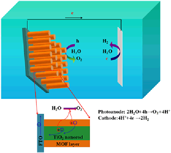
This paper presents a p-n heterojunction photoanode based on a p-type porphyrin metal-organic framework (MOF) thin film and an n-type rutile titanium dioxide nanorod array for photoelectrochemical water splitting. The TiO₂@MOF core-shell nanorod array is formed by coating an 8 nm thick MOF layer on a vertically aligned TiO2 nanorod array scaffold via a layer- by-layer self-assembly method. This vertically aligned core-shell nanorod array enables a long optical path length but a short path length for extraction of photogenerated minority charge carriers (holes) from TiO₂ to the electrolyte. A p-n junction is formed between TiO, and MOF, which improves the extraction of photogenerated electrons and holes out of the TiO₂ nanorods. In addition, the MOF coating significantly improves the efficiency of charge injection at the photoanode/electrolyte interface. Introduction of Co(III) into the MOF layer further enhances the charge extraction in the photoanode and improves the charge injection efficiency. As a result, the photoelectrochemical cell with the TiO₂@Co-MOF nanorod array photoanode exhibits a photocurrent density of 2.93 mA/cm² at 1.23 V (vs. RHE), which is ~ 2.7 times the photocurrent achieved with bare TiO2 nanorod array under irradiation of an unfiltered 300 W Xe lamp with an output power density of 100 mW/cm².
6. Gao, Xuefei, Zheng, Peng, Kasani, Sujan et.al. "Based surface-enhanced Raman scattering lateral flow strip for detection of neuron-specific enolase in blood plasma." Analytical chemistry 89.18 (2017): 10104-10110.
Abstract
An inexpensive and disposable paper-based lateral flow strip (PLFS) has been developed as an immunoassay, in which surface-enhanced Raman scattering (SERS) is utilized for sensing signal transduction. The Au nanostar@Raman Reporter@silica sandwich nanoparticles are developed as the SERS probes, which is the key to the high sensitivity of the device. Compared with a colorimetric PLFS, the SERS-PLFS exhibits superior performance in terms of sensitivity and limit of detection (LOD) in a blood plasma-containing sample matrix. In addition, the SERS-PLFS has been successfully used for detection of neuron-specific enolase (NSE), a traumatic brain injury (TBI) protein biomarker, in diluted blood plasma samples, achieving a LOD of 0.86 ng/mL. Moreover, the SERS-PLFS was successfully employed to measure the NSE level in clinical blood plasma samples taken from deidentified TBI patients. This work demonstrates that the SERS-PLFS has great potential in assisting screening of TBI patients in the point-of-care setting.
7. Zheng, Peng, Kasani, Sujan et al. "Detection of nitrite with a surface-enhanced Raman scattering sensor based on silver nanopyramid array." Analytica chimica acta 1040 (2018): 158-165.
Abstract
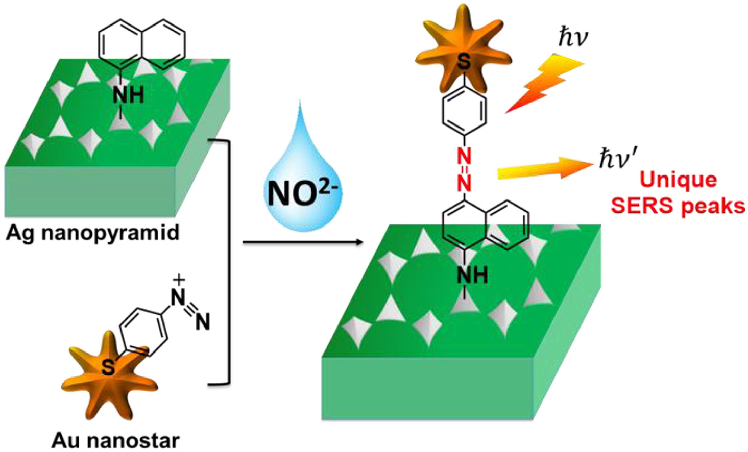
Nutrient pollution is of worldwide environmental and health concerns due to extensive use of nitrogen fertilizers and release of livestock waste, which induces nitrite compounds in aquatic systems. Herein a surface- enhanced Raman scattering (SERS) sensor is developed for nitrite detection based on coupling between the plasmonic gold nanostars and the silver nanopyramid array. When nitrite is present in the assay, an azo group is formed between the 1-naphthylamine-functionalized silver nanopyramids and the 4-aminothiophenol-functionalized gold nanostars. This not only generates the SERS spectral fingerprint for selective detection, but also creates "hot spots" at the gap between the Au nanostars and the Ag nanopyramids where the azo group is located, amplifying SERS signals remarkably. Finite-difference time-domain (FDTD) simulation shows a SERS enhancement factor of 4x10¹⁰ at the "hot spots". As a result, the SERS sensor achieves a limit of detection of 0.6 pg/mL toward nitrite in water, and enables nitrite detection in real-world river water samples. In addition, this sensor eliminates the use of any Raman reporter and any expensive molecular recognition probe such as antibody and aptamer. This highly sensitive, selective and inexpensive SERS sensor has unique advantages over colorimetric, electrochemical and fluorescent devices for small molecule detection.
8.Zheng, Peng, Kasani Sujan et al. "Origin of strong and narrow localized surface plasmon resonance of copper nanocubes." Nano Research 12.1 (2019): 63-68.
Abstract
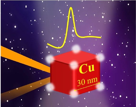
Inexpensive copper nanoparticles are generally thought to possess weak and broad localized surface plasmon resonance (LSPR). The present experimental and theoretical studies show that tailoring the Cu nanoparticle to a cubic shape results in a single intense, narrow, and asymmetric LSPR line shape, which is even superior to round-shaped gold nanoparticles. In this study, the dielectric function of copper is decomposed into an interband transition component and a free-electron component. This allows interband transition-induced plasmon damping to be visualized both spectrally and by surface polarization charges. The results reveal that the LSPR of Cu nanocubes originates from the corner mode as it is spectrally separated from the interband transitions. In addition, the interband transitions lead to severe damping of the local electromagnetic field but the cubic corner LSPR mode survives. Cu nanocubes display an extinction coefficient comparable to the dipole mode of a gold nanosphere with the same volume and show a larger local electromagnetic field enhancement. These results will guide development of inexpensive plasmonic copper-based nanomaterials.
9. Peng Zheng, Sujan Kasani, Weirui Tan, Jennifer Boryczka, Xuefei Gao, Feng Yang, Nianqiang Wu “Near-Infrared Fluorenscent Detection of Glial Fibrillary Acidic Protein in Blood Plasma Based on Gold Nano-pyramid Array”. Analytica Chimica Acta.

An ultrasensitive plasmonic near-infrared fluorescent biosensor substrate has been developed for detection of glial fibrillary acidic protein (GFAP) biomarker in blood plasma, an important protein biomarker of traumatic brain injury (TBI). To minimize the interference from blood plasma sample matrix, a near-infrared fluorophore in the first biological transparency window is used in the biosensor. To amplify the fluorescence signals, a plasmonic gold nanopyramid array has been coupled to the fluorophore. Finite-difference time-domain simulation reveals that the excitation enhancement is primarily responsible for the fluorescence enhancement owing to the intense local electric field excited on the corners and edges. As a result, this biosensor exhibits a lower limit of detection of 0.6 pg/mL toward detection of GFAP in blood plasma.
10. Hui Yang,Joeseph Bright, Banghao Chen, Peng Zheng, Xuefei Gao, Botong Liu, Sujan Kasani, Xiangwu Zhang, Nianqiang Wu “Chemical Interaction and Enhanced Interfacial Ion Transport in Ceramic Nanofiber-Polymer Composite Electrolyte for All-Solid-State Lithium Metal Battery”. Advanced Energy Materials.
Abstract

This paper reports the synergy between ceramic nanofibers and a polymer, and the enhanced interfacial Li-ion transport along the nanofiber/polymer interface in a solid-state ceramic/polymer composite electrolyte, in which a three-dimensional (3D) electrospun aluminum-doped Li0.33La0.557TiO3 (LLTO) nanofiber network is embedded in a polyvinylidene fluoride-hexafluoropropylene (PVDF-HFP) matrix. Strong chemical interaction occurs between the nanofibers and the polymer matrix. Addition of the ceramic nanofibers into the polymer matrix results in the dehydrofluorination of the PVDF chains, deprotonation of the –CH2 moiety and amorphization of the polymer matrix. Solid-state nuclear magnetic resonance (NMR) spectra reveal that lithium ions transport via three pathways: (i) intra-polymer transport, (ii) intra-nanofiber transport, and (iii) interfacial polymer/nanofiber transport. In addition, lithium phosphate is coated on the LLTO nanofiber surface before the nanofibers are embedded into the polymer matrix. The presence of lithium phosphate at the LLTO/polymer interface further enhances the chemical interaction between the nanofibers and the polymer, which promotes the lithium ion transport along the polymer/nanofiber interface. This in turn improves the ionic conductivity and electrochemical cycling stability of the nanofiber/polymer composite. As a result, the flexible LLTO/Li3PO4/polymer composite electrolyte membrane exhibits an ionic conductivity of 5.1 × 10⁻⁴ S cm−1 at room temperature and an electrochemical stability window of 5.0 V vs. Li/Li+. A symmetric Li|electrolyte|Li half-cell shows a low overpotential of 50 mV at a constant current density of 0.5 mA cm−2 for more than 800 h. In addition, a full cell is constructed by sandwiching the composite electrolyte between a lithium metal anode and a LiFePO4-based cathode. Such an all-solid-state lithium metal battery exhibits excellent cycling performance and rate capability.
11.Hui Yang, Botong Liu, Joeseph Bright, Sujan Kasani, Jianhui Yang, Xiangwu Zhang, Nianqiang Wu et al. "A Single-Ion Conducting UiO-66 Metal–Organic Framework Electrolyte for All-Solid-State Lithium Batteries
Abstract

A metal–organic framework (MOF) single lithium-ion conductor has been synthesized by covalently immobilizing anions to the skeleton of MOF structures. The functionalized UiO-66 MOF exhibits an electrochemical stability window of 5.2 V versus Li|Li+ and ionic conductivity of 6.0 × 10⁻⁵, 7.9 × 10⁻⁵, and 1.1 × 10⁻⁴ S/cm at 25, 60, and 90 °C, respectively. It displays single-ion conducting behavior with a high Li-ion transference number of 0.90 at 25 °C in the absence of any plasticizer. After ethylene carbonate and propylene carbonate are incorporated into the MOF structure, its ionic conductivity reaches 7.8 × 10⁻⁴ S/cm at room temperature. The MOF electrolyte has been evaluated with all-solid-state Li|MOF|LiFePO4 batteries at room temperature, showing excellent rate capacity and cycling stability.
12.Xuefei Gao, Jennifer Boryczka, Sujan Kasani, Nianqiang Wu "Enabling Direct Protein Detection in a Drop of Whole Blood with an “On-Strip” Plasma Separation Unit in a Paper-Based Lateral Flow Strip"
Abstract

Conventional paper lateral flow assays have low sensitivity and suffer from severe interference from complex human fluid sample matrices, which prevents their practical application in the testing of whole blood samples in the point-of-care settings. To solve this problem, gold nanostar@Raman reporter@silica-sandwiched nanoparticles have been developed as the surface-enhanced Raman scattering (SERS) probes for sensing transduction; and a functionalized filter membrane assembly has been designed and constructed in the paper-based lateral flow strip (PLFS) as a built-in plasma separation unit. In this “on-strip” plasma separation unit, three layers of filter membranes are stacked and surface-modified to maximize the separation efficiency and the plasma yield. As a result, the integrated PLFS has been successfully used for the detection of carcinoembryonic antigen (CEA) in 30 μL of whole blood with the assistance of a portable Raman reader, achieving a limit of detection of 1.0 ng mL–1. In short, this report presents an inexpensive, disposable, portable, and field-deployable paper-based device as a general point-of-care testing tool for protein biomarker detection in a drop of whole blood.
13.Xuefei Gao, Jennifer Boryczka, Peng Zheng, Sujan Kasani, Feng Yang, Elizabeth B Engler-Chiurazzi, James W Simpkins, Jane G Wigginton, Nianqiang Wu"A “hot Spot”-Enhanced paper lateral flow assay for ultrasensitive detection of traumatic brain injury biomarker S-100β in blood plasma"
Abstract
Currently colorimetric paper lateral flow strips (PLFS) encounter two major limitations, that is, low sensitivity and severe interference from complex sample matrices such as blood. These shortcomings limit their application in detection of low-concentration analytes in complex samples. To solve these problems, a PLFS has been developed by utilizing surface-enhanced Raman scattering (SERS) for sensing signal transduction. In particular, a hierarchical three-dimensional nanostructure has been designed to create “hot spots”, which can significantly amplify the SERS sensing signal, leading to high sensitivity. As a result, this PLFS has demonstrated a limit of detection (LOD) of 5.0 pg mL−1 toward detection of S-100β, a traumatic brain injury (TBI) protein biomarker in blood plasma. The PLFS has been successfully used for rapid measurement of S-100β in clinical TBI patient samples taken in the emergency department. Availability of PLFS for blood testing would shift the paradigm of TBI patient management and clinical outcome in emergency departments. It is expected that this type of PLFS can be adapted for rapid detection of various human diseases due to its capability of measuring a low level of protein blood biomarkers in complex human fluids.
14.P Zheng,S Kasani,N Wu"Converting plasmonic light scattering to confined light absorption and creating plexcitons by coupling a gold nano-pyramid array onto a silica–gold film"
Abstract

This report presents a facile microfabrication-compatible approach to fabricate a large area of plasmonic nano-pyramid array-based antennas and demonstrates effective light management by tailoring the architecture. First, a long-range ordered gold nano-pyramid array is fabricated, which exhibits strong light scattering. The maximum electric field enhancement (|E|/|E0|) of 271 is achieved at the corner but decays rapidly away from the pyramid bottom. After the gold nanopyramid array is coupled to a gold film, strong light scattering is converted into strong light absorption due to the excitation of a spectrally tunable plasmonic gap mode, where an intense electric field enhancement of 233 and a strong magnetic field enhancement (|H|/|H0|) of 25 are simultaneously excited for a 10 nm silica gap. The electric field decays much slower away from the pyramid bottom while the magnetic field keeps almost constant. In addition, both experiments and finite-difference time-domain (FDTD) simulations have confirmed that strong plasmon–exciton coupling between the plasmonic gap mode and the J-aggregates can take place when quantum emitters such as J-aggregates are embedded in the gap, creating plexcitons. This can overcome the problems of high energy loss and weak nonlinearity, which are typically associated with surface plasmon polaritons (SPPs) supported on plasmonic metallic nanostructures. The coherent plasmon–exciton coupling (plexciton) generated by the film-coupled nano-pyramid nanostructure is expected to find promising applications in light-emitting devices, photodetectors, photovoltaics and photoelectrochemical cells.
15.Xiaoyan Cai, Liang Mao, Mamoru Fujitsuka, Tetsuro Majima, Sujan Kasani, Nianqiang Wu, Junying Zhang"Effects of Bi-dopant and co-catalysts upon hole surface trapping on La2Ti2O7 nanosheet photocatalysts in overall solar water splitting"
Abstract
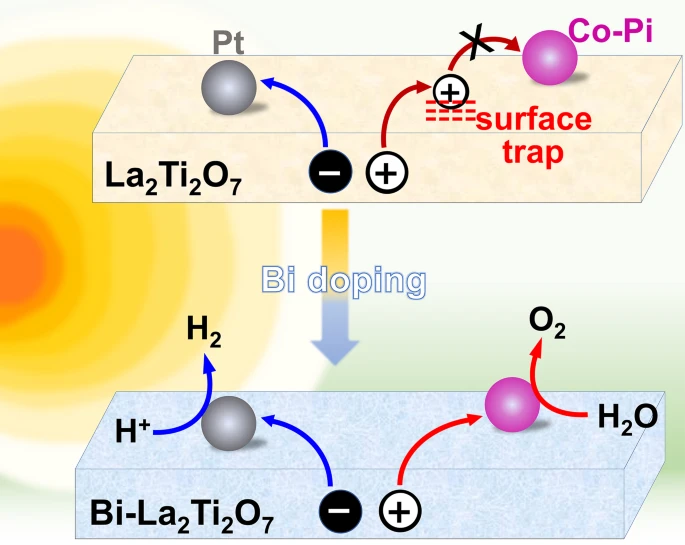
Pristine and Bi-doped lanthanum titanium oxide (La2Ti2O7) nanosheets have been synthesized as photocatalysts for overall solar water splitting. The surface hole trap is a critical factor that limits the photocatalytic activity of pristine La2Ti2O7. Deposition of cobalt phosphate (Co-Pi) and platinum (Pt) nanoparticles on La2Ti2O7 cannot remove the surface traps although they are essential for enabling the oxygen and hydrogen evolution reactions. It is interesting that doping bismuth (Bi) into La2Ti2O7 nanosheets has eliminated the surface traps due to surface enrichment of Bi. The Co-Pi/Bi-La2Ti2O7/Pt nanosheets exhibit increasing photocatalytic activity toward overall water splitting with increasing the Bi-dopant level up to 5 at.%. Further increasing the Bi-dopant level leads to the formation of localized states above the valence band, leading to the lifetime reduction of photogenerated charge-carriers, and jeopardizing the photocatalytic activity. This work proposes an effective strategy to address the surface trapping and surface catalysis issues in the nanostructured metal oxide photocatalysts.
16.Hui Yang, Kieran Tay, Yaobin Xu, Biplab Rajbanshi, Sujan Kasani, Joeseph Bright, Jennifer Boryczka, Chongmin Wang, Peng Bai, Nianqiang Wu"Nitrogen-Doped Lithium Lanthanum Titanate Nanofiber-Polymer Composite Electrolytes for All-Solid-State Lithium Batteries"
Abstract
Currently cation doping is common for improving ionic conductivity of metal oxide-based lithium-ion conductors. In this work, anions (nitrogen ions) have been doped to perovskite Li3xLa2/3 − xTiO3 (LLTO) nanofibers by heat treatment in the ammonia-containing atmosphere, and substituted for oxygen anions partially in the perovskite structure. Density-functional theory (DFT) calculation results reveal that nitrogen doping weakens the bonding of Li ions on the A sites in perovskite ABO3 structure and allows for larger lattice distortion, reducing the activation energy for Li-ion hopping in both the forward and backward jumping directions. Experimental results have also confirmed that nitrogen doping has improved ionic conductivity of LLTO. Nitrogen-doped LLTO nanofibers have been incorporated with a poly (vinylidene fluoride)-co-hexafluoropropylene (PVDF-HFP) polymer to form a solid-state composite electrolyte, which exhibits ionic conductivity of 3.8 × 10⁻⁴ S·cm−1 at room temperature and an electrochemical stability window of up to 4.9 V vs Li∣Li+. The all-solid-state Li metal∣composite electrolyte∣LiFePO4 lithium batteries, which employ nitrogen-doped LLTO nanofibers, show better rate capability and cycling stability at room temperature than the counterparts with pristine LLTO nanofibers.
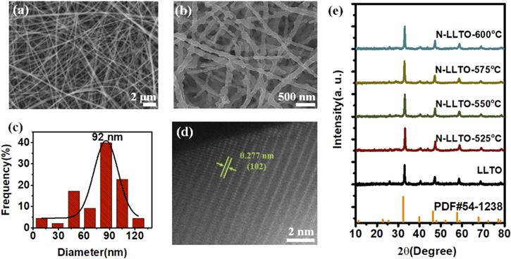
17.Sasanka Katreddi, Sujan Kasani, Arvind Thiruvengadam"A Review of Applications of Artificial Intelligence in Heavy Duty Trucks"
Abstract
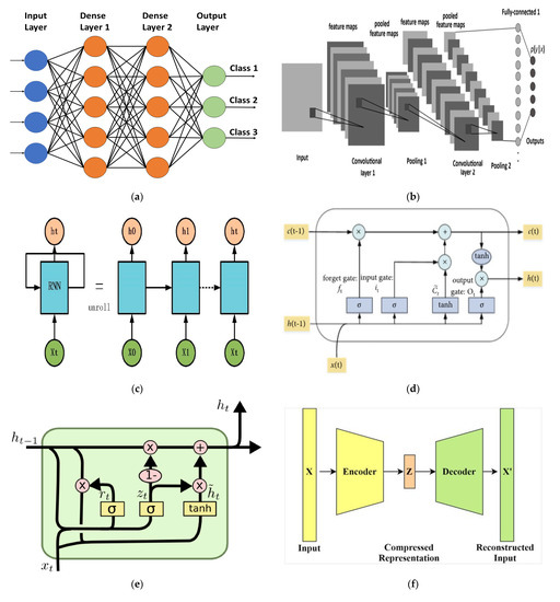
Due to the increasing use of automobiles, the transportation industry is facing challenges of increased emissions, driver safety concerns, travel demand, etc. Hence, automotive industries are manufacturing vehicles that produce fewer emissions, are fuel-efficient, and provide safety for drivers. Artificial intelligence has taken a major leap recently and provides unprecedented opportunities to enhance performance, including in the automotive and transportation sectors. Artificial intelligence shows promising results in the trucking industry for increasing productivity, sustainability, reliability, and safety. Compared to passenger vehicles, heavy-duty vehicles present challenges due to their larger dimensions/weight and require attention to dynamics during operation. Data collected from vehicles can be used for emission and fuel consumption testing, as the drive cycle data represent real-world operating characteristics based on heavy-duty vehicles and their vocational use. Understanding the activity profiles of heavy-duty vehicles is important for freight companies to meet fuel consumption and emission standards, prevent unwanted downtime, and ensure the safety of drivers. Utilizing the large amount of data being collected these days and advanced computational methods such as artificial intelligence can help obtain insights in less time without on-road testing. However, the availability of data and the ability to apply data analysis/machine learning methods on heavy-duty vehicles have room for improvement in areas such as autonomous trucks, connected vehicles, predictive maintenance, fault diagnosis, etc. This paper presents a review of work on artificial intelligence, recent advancements, and research challenges in the trucking industry. Different applications of artificial intelligence in heavy-duty trucks, such as fuel consumption prediction, emissions estimation, self-driving technology, and predictive maintenance using various machine learning and deep learning methods, are discussed.
18.Sujan Phani Kumar Kasani"Characterization of Defects on MOCVD Grown Gallium Nitride Using Transient Analysis Techniques"
Abstract
Since the invention of the first visible spectrum (red) LED by Holonyak in 1962, there has been a need for more efficient, more reliable and less expensive LEDs. The III-nitrides revolutionized semiconductor technology with their applications in the blue LED’s. However the internal quantum efficiency of LED’s are limited by the deep level traps in GaN substrate. Traps are defects in the crystal lattice, which depends on growth parameters. These traps act as non radiative centers where non-radiative recombination occurs without conversion of available energy into light. Characterization of these traps in a material is necessary for better understanding of the material growth quality and resulting device performance. In this work Capacitance-Voltage (C-V) and Deep Level Transient Spectroscopy (DLTS) are conducted which provide electronic properties of trap centers like activation energy, doping concentration and capture cross-section. In n-GaN grown by Metalorganic Chemical Vapor Deposition (MOCVD) on Sapphire two defects types are detected and are characterized by Capacitance Voltage and Deep Level Transient Spectroscopy. Two deep levels E1 and E2 are typically observed in n-GaN with the activation energies of 0.21eV and 0.53eV at 125°K and 325°K, respectively. The deep level E1 is caused by linear line defects along dislocation cores while deep level E2 is related to point defects. The characterization techniques, experimental systems and preliminary characterization results are discussed in detail.
19.Sujan Phani Kumar Kasani, Mani Manivannan"Surface Photo-Voltage (SPV) and Photo electrochemistry (PEC) on TiO2"
Abstract
Hydrothermally grown rutile titanium dioxide (TiO2) nanorod array photoanode with various nanorod lengths were investigated for understanding the charge carrier separation including hole diffusion length using Photoelectrochemistry (PEC) and surface photo voltage (SPV) measurements for their importance in photoconversion as photoelectrode for solar water splitting. Various lengths of TiO2 nanorods with lengths 1.35, 1.85, 2.5 and 4.5 micrometers were prepared and used in the present investigation. Front and back illumination in SPV and PEC Mott-Schottky plots were investigated and found to show significant difference in charge carrier separation. The hole diffusion length calculations using PEC was up to 200 nm and using SPV was in the order of 600-700nm.
Conferences
1. Strong Coupling under Gap Plasmon Mode in a Film-Gold Nanopyramid Array Structure. Sujan Kasani and Nianqiang Wu. Materials Research Society, 2018.
2. Plasmonic nano-ring array for Surface Enhanced Raman Scattering. Sujan Kasani, Peng Zheng, Nianqiang Wu; ACMAE symposium, West Virginia University, April 20, 2018.
3. Optimizing a long range highly ordered plasmonic nanoarray pattern for Surface-Enhanced Raman Scattering, Sujan Kasani, Peng Zheng, Nianqiang Wu; Electrochemical Society Conference, 2017.
4. Tunable localized surface plasmon resonance in transition metal oxide nanostructures. Sujan Kasani and Nianqiang Wu, Nanostructured Materials and Nano Chemistry, 2018.
5. Gap mode 3D nano structure supporting strong coupling regime for improving optoelectronic device performance. Sujan Kasani, Peng Zheng and Nianqiang Wu, Nanotechnology and Expo, 2018.
6. Plasmonic Nanostructures for Early Disease Detection and Precision Cancer Therapeutics, Kathrine Curtin, Sujan Kasani, Nianqiang Wu; Electrochemical Society Conference, 2019.
7. Fabrication of Hierarchical Nanostructures for Surface-Enhanced Raman Scattering Biosensors, Kathrine Curtin, Sujan Kasani, Nianqiang Wu; Electrochemical Society Conference, 2017.
8. A Paper-Based Surface-Enhanced Raman Scattering Test Strip for Protein Biomarker Detection by Xuefei Gao, Peng Zheng, Sujan Kasani, Nianqiang Wu, Electrochemical Society Conference, 2017.
9. Monitoring Contaminants in Aquatic Environment with Portable Sensors, Peng Zheng, Xuefei Gao, Sujan Kasani, Nianqiang Wu, West Virginia University Institute of Water Security and Science Spring Symposium, 2017.
10. Fabrication of Hierarchical Nanostructures for Surface-Enhanced Raman Scattering Biosensors Kathrine Curtin, Sujan Kasani, Peng Zheng, Nianqiang Wu, Summer Undergraduate Research Symposium, West Virginia University, July 28, 2016.
Contact
Hillsboro OR 97006